Overview
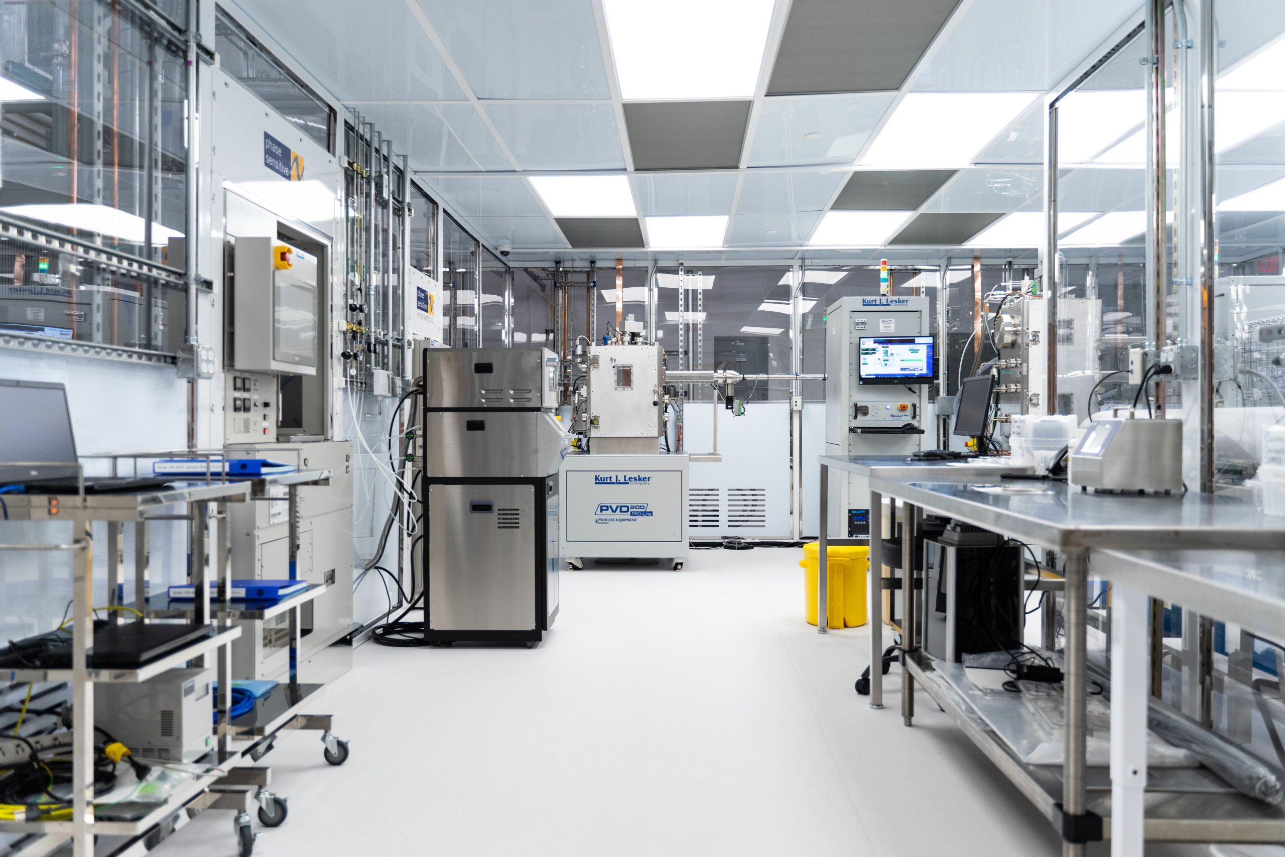
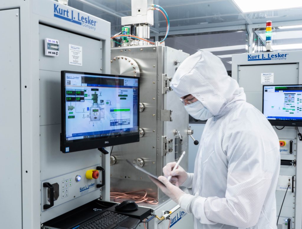
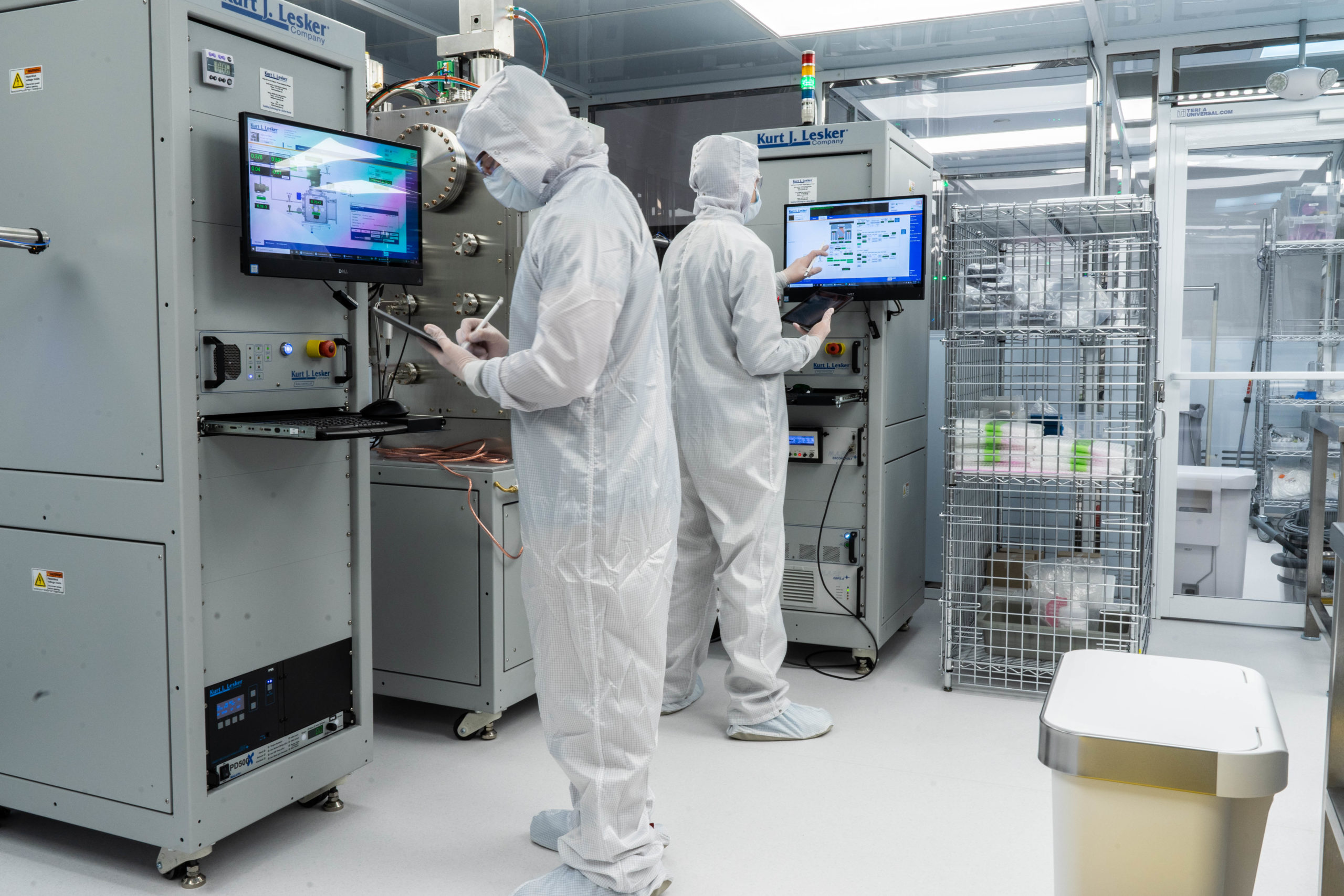
PSI has the required design and modeling software to aid in the support of custom photonic device designs, providing an in-house support to PSI’s photonic device fabrication capabilities. PSI has 2000+ sqft of cleanroom and conditioned laboratory space dedicated to the fabrication of RF and RF Photonic devices. Consulting services for photonic device design and fabrication are available, in addition to a full design through fabrication service. Design and fabrication services can range from consulting, bare die fabrication or extend to packaged die services, based on your requirements.
Capabilities
- Access to commercially licensed design suites for RF photonic devices, in addition to PSI’s proprietary design toolboxes.
- Microfabrication cleanroom with 1200 sqft of an ISO 6 and ISO 7 class cleanroom with processing equipment capabilities for up to 6” diameter wafers.
- 1000+ sqft of lab space dedicated for mid- to back-end wafer processing, allowing the evaluation, singulation and assembly of RF and photonic dies.
- PSI has performed custom RF photonic device design solutions, supplying bare die modulators, arrayed high-speed phase modulators, custom waveguide and RF Photonic devices.

